GLSUN - 20+ Years' Professional Manufacturer


Fiber Optic Tech
Spectral Detection of Laser Chips
June 29,2024
A laser chip is a type of semiconductor device that uses semiconductor material as the gain medium and employs electrical pumping to generate laser light. Because its gain is typically produced by the current flowing through the p-n junction or p-i-n junction, it is also known as a laser diode (LD).
Laser chips offer significant advantages, including high efficiency, compact size, high reliability, long lifespan, wide wavelength range, and high modulation rate. As core components, they can be integrated into various lasers and optical systems such as fiber lasers, solid-state lasers, and lidar. The application fields are extensive. From the perspective of utilizing laser photons, these applications can be categorized into two types: energy photons and information photons. The specific details are shown in the table below.
Photon Type |
Laser Type |
Applications |
Energy Photon |
Fiber-optic Laser |
Marking, engraving, cutting, welding, metal 3D printing and other material processing fields, applied to aerospace, automobile manufacturing, shipbuilding, steel metallurgy, 3C electronics, national defense, etc. |
Solid-state and ultrafast Lasers |
Precision cutting, punching, stripping, removal, dicing, resistance and frequency modulation, micro-nano structure processing, applied to semiconductor microelectronics, display panels and lighting, aerospace, automobiles, solar energy, 3C electronics, 3D additive manufacturing, etc. |
|
Direct Semiconductor Lasers |
Welding, cladding, quenching, surface heat treatment, used in automobile manufacturing, power generation equipment, 3C electronics, aerospace, high-speed rail, steel metallurgy, etc. |
|
Biomedical Lasers |
Medical aesthetics, Physiotherapy,Surgery, Photodynamic therapy |
|
Directional Lasers |
Scientific Research and Military |
|
Information Photonics |
Optical Communication Lasers |
Access network, backbone network, data center, 5G, Internet of Things(IoT) |
Silicon Photonic Chip |
Data Transmission and Processing |
|
Laser Lidar |
3D facial recognition and auxiliary imaging, detection and tracking, security monitoring, autonomous driving, machine vision, distance measurement, and precise measurement |
|
Sensor |
Sensors for substances such as liquids and gases, proximity sensors, etc. |
|
Mid-infrared and far-infrared, terahertz lasers |
Detection and Imaging, Electro-Optical Countermeasures |
|
Red, Green, and Blue Lasers |
Laser TVs, Laser Projectors, Automotive Headlights, Laser Lighting, etc. |
Applications of Laser Chips
Structurally, a laser chip resembles a multi-layered cake. At its core is the active layer, flanked on either side by n-type and p-type cladding layers. Below these layers lie the substrate and electrode, while above them are the cap layer and electrode. Carriers injected from the electrodes on either side recombine in the active layer, emitting photons. The difference in refractive indices between the active layer and the adjacent layers results in a waveguide effect, confining the photons within this waveguide layer. Mirrors are then formed through end-face coating, creating a resonant cavity that provides positive feedback for energy, ultimately producing laser light.
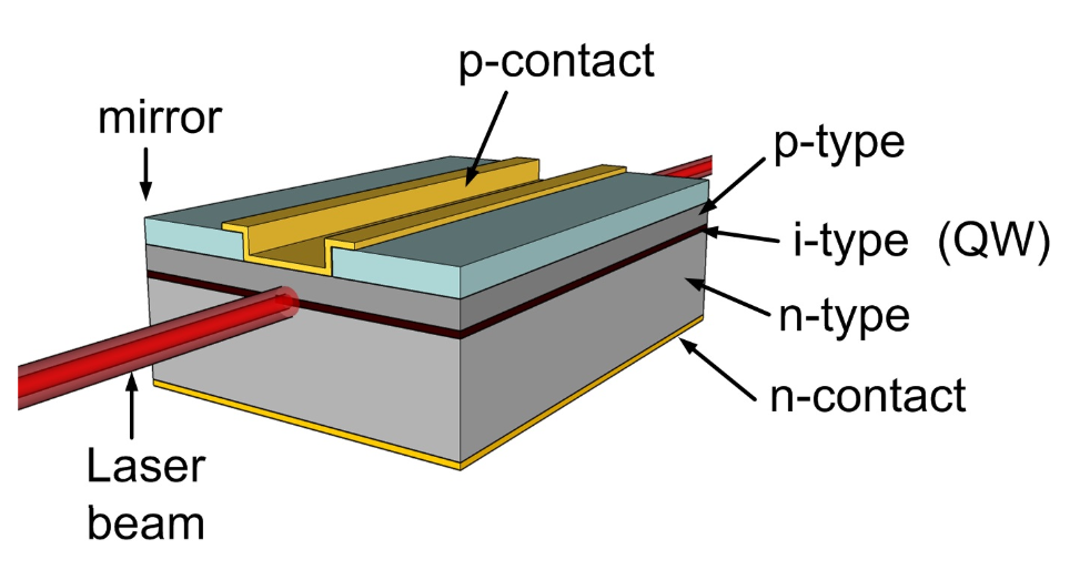
Structure Diagram of Laser Chip
The generation of laser photons originates from the recombination of carriers in the active layer, hence their wavelength is determined by the bandgap of semiconductor materials in the active layer. Commonly used materials include compound semiconductors with direct bandgaps, such as AlGaAs, InGaAs, and InGaAsP. The abundance of semiconductor materials provides the foundation and possibility to cover a wide spectral range. By changing the types of elements in the compound, a wide range of wavelength adjustments can be achieved, while fine-tuning of the wavelength can be accomplished by varying the proportions of the elements.
Active Layer |
Substrate |
Typ. Excitation Wavelength |
InGaN |
GaN |
380-540nm |
AIGaInP |
GaAs |
620-700nm |
AIGaAs |
GaAs |
720-850nm |
InGaAs |
GaAs |
900-1100nm |
InGaAsP |
InP |
1200-2000nm |
AIGaAsSb |
GaSb |
1800-3400nm |
Laser chip materials and wavelengths
According to the emission method, laser chips are divided into Edge Emitting Lasers (EEL) and Surface Emitting Lasers. Currently, a typical representative of Surface Emitting Lasers is the Vertical Cavity Surface Emitting Laser (VCSEL). Edge Emitting Lasers have optical coatings on both side facets forming a resonant cavity, emitting laser light along a direction parallel to the substrate surface. In contrast, the resonant cavity of VCSELs is located on the top and bottom sides, emitting laser light along a direction perpendicular to the substrate surface.
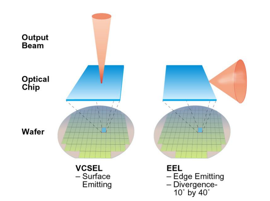
Schematic diagrams of surface emitting and edge emitting laser chips
The detailed comparison of the two types of laser chips is shown in the following table. It can be seen that EEL has the advantage of higher power density but suffers from poorer beam quality, which is not conducive to beam shaping. VCSEL, on the other hand, excels in better beam quality and is easier for two-dimensional integration, but has the drawback of lower power density.
Item |
EEL |
VCSEL |
Spot Shape |
Oval |
Round |
Divergence Angle |
Large |
Small |
Spectral Broadband |
1-10 nm |
1 nm |
Wavelength Temperature Stability |
0.07-0.3 nm/℃ |
0.07 nm/℃ |
Power Density |
High |
Low |
Photoelectric Conversion Efficiency |
Low |
High |
Cost |
High |
Low |
EEL vs VCSEL
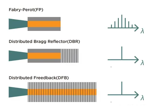
Edge-emitting laser chips can be further classified into three types based on the different structures of their resonators: Fabry-Perot (FP) laser chips, distributed Bragg reflector (DBR) laser chips, and distributed feedback (DFB) laser chips.
The resonant cavity of an FP laser chip is a Fabry–Perot (FP) cavity. This is the most common type of laser chip, particularly prent in high-power applications. However, its emitted laser is multi-longitudinal mode with a relatively wide bandwidth, which limits its use in many other fields, such as communications. To achieve single-longitudinal-mode output, grating feedback must be incorporated into the chip structure. When the grating structure is integrated along the entire resonant cavity, it forms a distributed feedback (DFB) laser chip. If the grating structure acts as an end mirror placed at the side of the resonant cavity, it forms a distributed Bragg reflector (DBR) laser chip. In DFB and DBR laser chips, the grating structure allows for the selection of single-longitudinal-mode laser output, as shown in the diagram below.
Surface-emitting laser chips also have subcategories, such as the emerging Photonic Crystal Surface Emitting Laser (PCSEL). This type uses a two-dimensional photonic crystal as the emitting surface, and through the design of the photonic band structure, it achieves laser mode selection and angle control. It features an extremely small beam divergence angle (≤1°), demonstrating excellent application potential.
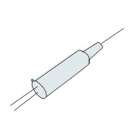
Laser chips are precision optoelectronic devices manufactured using semiconductor chip fabrication processes. The manufacturing process of a typical edge-emitting laser chip, as shown in the diagram below, mainly includes the following steps: design, epitaxial growth, wafer fabrication, cleaving, coating, packaging, and testing.
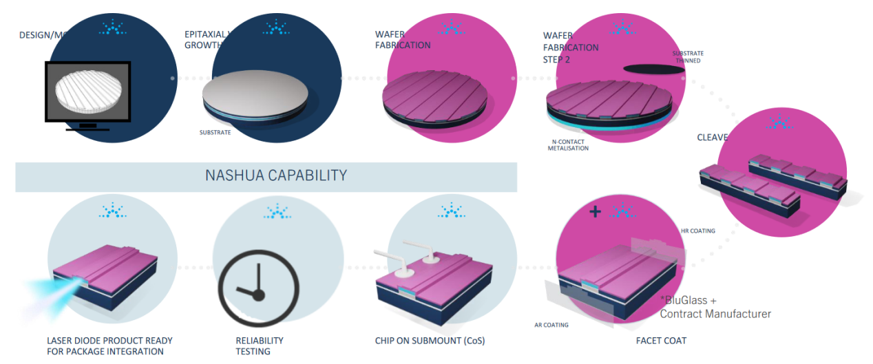
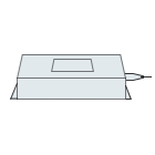
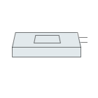
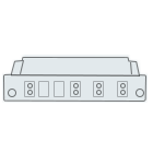
Once packaged, laser chips serve as core components, enabling controlled laser output when combined with optical, mechanical, power, and control systems. This allows their use in fields such as laser processing, communications, and sensing. The performance parameters of laser chips, such as output power, spectrum, and beam quality, are crucial for their applications. Therefore, parameter testing is an essential part of the laser chip manufacturing process and quality control.


