

















Fiber Optic Tech
Optical Packaging Technologies Explained: Why Precision Determines Performance
In the era of rapid development in high-speed optical communications, data centers, 5G/6G networks, and silicon photonics integrated circuits, Optical Packaging Technology has become the core factor determining the overall performance of optical devices. From Laser Diode and Photodiode to complete Optical Modules, the packaging process not only protects the chips from external environmental influences but also directly affects optical signal transmission efficiency, stability, and reliability. This article provides an in-depth analysis of the core concepts, key processes, common technology comparisons, and how precision alignment determines final performance in optical packaging. It also highlights GLSUN’s one-stop manufacturing capabilities in optical packaging solutions.
What Is Optical Packaging?
Optical Packaging refers to the process of assembling optoelectronic devices (such as laser chips, photodetectors, waveguides, etc.) with optical fibers, lenses, or other optical components to form stable, commercially viable optoelectronic assemblies or modules. Unlike traditional electronic packaging, it requires simultaneous consideration of electrical, thermal, optical, and mechanical multidisciplinary coupling.
The Optical Packaging Process typically includes chip mounting, heat sink design, fiber/waveguide alignment, sealing protection, electrical interconnection, and performance testing. High-quality Optical Packaging Solutions can significantly reduce Insertion Loss, improve Return Loss, and ensure long-term reliability of devices in harsh environments.
Common optical packaging product forms include:
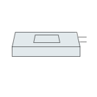
· Fiber Array: Used for multi-channel high-density optical coupling and a key component in silicon photonics and high-speed optical modules.
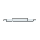
· Optical Isolator: Prevents reflected light from feeding back into the laser source, protecting system stability.
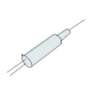
Laser Diode and Photodiode packaged modules.
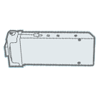
Complete Optical Modules, such as 400G/800G transceivers.
Why Does Packaging Precision Directly Affect Performance?
Optical signals typically operate at wavelengths around 1310nm or 1550nm, with mode field diameters of only a few micrometers or even sub-micrometers. Any minor positional deviation, angular tilt, or thermal expansion mismatch can cause a sharp drop in optical coupling efficiency. Packaging precision directly determines:
· Coupling Efficiency: Sub-micron deviations can lead to additional losses exceeding 3dB.
· Signal Integrity: High-precision packaging minimizes reflections and reduces noise.
· Thermal Management and Reliability: Precise heat sink and sealing designs ensure stable chip operation under high power.
· Long-term Stability: Prevents alignment drift caused by humidity, vibration, or temperature cycling.
In the silicon photonics era, packaging precision has become a bottleneck constraining system bandwidth and transmission distance. Advanced Optical Packaging Technology is the key to breaking through this bottleneck.
Comparison of Common Packaging Technologies
1. TO CAN Packaging
TO CAN (Transistor Outline Can) is the most traditional metal can-style packaging, commonly used for low-speed or medium-to-low power lasers and detectors. It features a simple structure, low cost, and good heat dissipation but has limited alignment precision. It is suitable for single-channel or low-density applications. Its drawbacks include larger size, which is unfavorable for high-density integration, and higher parasitic inductance in high-speed applications.
2. COB (Chip on Board) Packaging
COB technology mounts chips directly onto the circuit board, achieves electrical connections via wire bonding, and then performs fiber alignment and protection. This approach offers high cost-effectiveness and is suitable for mid-to-low-end optical modules. However, due to the lack of precise mechanical references, alignment consistency is poorer in high-channel-count or silicon photonics applications.
3. Butterfly Packaging
Butterfly packaging uses ceramic or metal substrates to provide excellent thermal management and RF performance. It is commonly used in high-power lasers, Erbium-Doped Fiber Amplifier (EDFA) modules, and research instruments. It supports multi-pin, high-reliability sealing and is suitable for applications requiring precise temperature control. The volume is moderate, but assembly complexity is higher.
4. Silicon Photonics Packaging
This is currently the most advanced technology, focusing on the co-packaging of Photonic Integrated Circuits (PICs) with optical fibers and electronic chips. Silicon Photonics Packaging emphasizes high-density, multi-channel coupling, often combined with Fiber Array using edge coupling or grating coupling methods. It achieves extremely high integration levels and supports 400G/800G and higher speeds, but it places extremely high demands on packaging precision and process consistency. It is the mainstream direction for future data center and AI computing optical interconnects.
Comparison Summary: TO CAN and COB focus more on cost, Butterfly emphasizes reliability and power handling, while Silicon Photonics Packaging pursues ultimate integration and performance. The choice of Optical Packaging Technology depends on the application scenario, cost budget, and performance requirements.
Fiber Alignment Technologies: Active Alignment vs. Passive Alignment
Fiber alignment is the most challenging step in optical packaging and directly affects coupling efficiency.
· Active Alignment: During the packaging process, optical power is monitored in real time, and a precision six-degree-of-freedom adjustment platform dynamically adjusts the position of the fiber or chip until optimal coupling is achieved. Its advantages are the highest precision (sub-micron or even nanometer level) and strong adaptability, making it suitable for high-performance products such as premium Optical Modules and silicon photonics devices. However, the process is time-consuming and equipment costs are high, so it is more suitable for medium-to-low volume production or high-value products.
· Passive Alignment: This relies on pre-machined mechanical references (such as V-grooves, alignment pins, or visual marks) to achieve "plug-and-play" assembly. No real-time feedback is required, resulting in fast speed, low cost, and ease of automation for mass production. However, precision is limited by manufacturing tolerances, making it suitable for Fiber Array or standardized products with high consistency requirements.
Hybrid alignment strategies are becoming a trend: critical channels use active alignment, while others leverage passive references. GLSUN combines both technologies in actual production to provide customers with optimized solutions that balance performance and cost.
Impact of Packaging on Insertion Loss, Return Loss, and Reliability
· Insertion Loss: Refers to the power attenuation of the optical signal passing through the device. Precision packaging can control the insertion loss of multi-channel Fiber Array at extremely low levels (e.g., <0.5dB per channel). Alignment deviations significantly increase loss, affecting transmission distance and system budget.
· Return Loss: Measures the suppression of reflected light. High return loss (typically >50dB) prevents reflected light from interfering with laser operation. Optical Isolator plays a key role here. GLSUN’s high-power optical isolators provide excellent protection in reflective environments.
· Reliability: Precision packaging uses advanced sealing processes (such as laser welding and epoxy curing) and thermal expansion-matched materials to ensure devices pass stringent reliability tests such as Telcordia GR-468. Performance remains stable under extreme temperature, humidity, or vibration conditions.
GLSUN’s One-Stop Manufacturing Capability from Chip to Packaging
As a professional manufacturer in the optical device field, GLSUN possesses one-stop manufacturing capabilities ranging from chip design and wafer processing to complete packaging and testing. We are proficient in various Optical Packaging Processes and can provide customers with customized Optical Packaging Solutions.
· Fiber Array: Offers high-precision solutions including MT-FA, multi-channel (4CH/8CH), Z-block, and more to meet the high-density requirements of silicon photonics packaging.
· Optical Isolator: Single-channel, array-type, high-power free-space, and in-line isolators, widely used in laser protection and optical amplification systems.
· Laser Diode & Photodiode modules: High-reliability packaging ensuring excellent optoelectronic performance.
· Optical Modules: From sub-assemblies to complete modules, supporting high-speed data center applications.
GLSUN’s packaging facilities are equipped with advanced active/passive alignment equipment, cleanroom environments, and fully automated testing systems, enabling seamless transitions from prototype development to mass production. Whether it is TO CAN, Butterfly, or Silicon Photonics Packaging, we deliver high-consistency, high-yield products to help customers accelerate time-to-market.
Precision Packaging Illuminates the Future of Optical Communications
Optical Packaging Technology is undergoing a critical transformation from a supporting role to a core competitive advantage. Packaging precision is no longer merely a process issue but a strategic element that directly determines the performance, cost, and reliability of Optical Modules. With the popularization of silicon photonics technology, demand for high-precision, multi-functional Optical Packaging Solutions will continue to surge.
Choosing a partner with a complete industry chain and rich experience is crucial. GLSUN is committed to providing global customers with full-chain solutions from chip to system through innovative Optical Packaging Technology. If you are looking for high-performance Fiber Array, optical isolators, or custom optical modules, please contact the GLSUN professional team to explore the infinite possibilities of next-generation optical interconnects together.


