


Fiber Optic Tech
In-depth Analysis of OCS Diversified Solutions and Their Profound Impact on the Optical Transceiver Market
In an era of explosive data growth, optical communication networks are facing unprecedented bandwidth pressure and energy consumption challenges. Optical Circuit Switching (OCS), as a revolutionary network architecture, is quietly reshaping the competitive landscape of the entire optical communications industry. It is no longer a single technical path but a convergence and competition among multiple cutting-edge physical implementations. These solutions differ not only in their technical characteristics but also in application scenarios, reliability, and scalability, driving the optical communications industry chain to evolve from traditional “point-to-point” transmission toward intelligent, integrated all-optical networks. This article starts with a comparison of technical solutions, deeply analyzes the four core paths of OCS, and explores their profound impact on the optical transceiver market, revealing how the industry focus is shifting from “quantity” expansion to “quality” leaps.
I. The Competition Among Four Major Technical Paths: A Comprehensive Comparison from Physical Principles to Scenario Adaptation
The core of OCS lies in achieving direct switching of optical signals without electrical domain conversion, significantly reducing latency, power consumption, and costs. However, the paths to achieve this goal vary greatly. The current mainstream four solutions—MEMS, DLC, DBS (or DLBS), and optical waveguide—are in fierce technical competition, each embodying the evolutionary logic of optical communications from microscopic physics to macroscopic system integration.
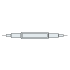
First, the MEMS (Micro-Electro-Mechanical Systems) solution has become the mainstream choice for current data centers. Its core principle involves using silicon-based micro-mirror arrays to precisely control beam direction. By integrating thousands or even tens of thousands of micro-mirrors on a silicon wafer, MEMS devices can achieve micron-level angular deflection under electrical signal drive, enabling dynamic optical path switching. The advantages of this solution include high precision and high reliability: mirror array response times reach millisecond levels, insertion loss is as low as 1-2 dB, and it performs excellently in high-temperature and high-humidity environments. Leading hyperscale data center operators such as Google, Microsoft, and others have deployed MEMS-based OCS systems at scale for internal interconnect traffic scheduling. For example, in hyperscale data centers, MEMS OCS can seamlessly reconfigure hundreds of rack-level fiber links to support dynamic bandwidth al for AI training clusters. Compared to traditional electrical switches, its power consumption can be reduced by over 90%, with higher port density. However, MEMS has drawbacks such as potential fatigue risks from mechanical components and complex manufacturing processes—silicon micro-machining requires extremely high cleanliness and precision, leading to higher initial costs. Nevertheless, with iterations in semiconductor processes (such as 7nm-level silicon etching), MEMS reliability has approached “zero-failure” levels, making it the preferred choice for “zero-interruption” operations in data centers. Recent deployments, including products from Lumentum (R300), DiCon (300x300 and 64x64 models), and Eoptolink (NX200/NX300), continue to dominate AI data center applications with low end-to-end loss (<3.0 dB) and proven long-term field reliability.
Second, the DLC (Digital Liquid Crystal) solution stands out for its extremely low drive voltage and superior environmental adaptability. The core principle relies on electric fields to regulate liquid crystal molecular alignment, thereby changing the refractive index path of optical signals. When a voltage below 10V is applied to the liquid crystal layer, beam deflection or blocking can be achieved entirely through electro-optic effects, with no mechanical movement. This gives DLC devices exceptional reliability: no moving parts, far superior vibration and shock resistance compared to MEMS, making it particularly suitable for extreme environments such as submarine cable networks or military communications. In submarine cables, DLC OCS can withstand thousands of meters of water pressure and temperature fluctuations from -20°C to +80°C, with lifespans exceeding 25 years. In technical comparison, DLC features simple drive circuits, power consumption only one-third that of MEMS, and excellent temperature stability (refractive index variation <0.01% with temperature). However, its response speed is slightly slower than MEMS (approximately 10-50 ms), and the material is more sensitive to wavelength, mainly suitable for medium-to-low-speed switching in WDM systems. Nevertheless, in global submarine cable projects, DLC has proven irreplaceable in “long-life, low-maintenance” scenarios, extending optical communications from terrestrial data centers to oceans, space, and other extreme domains. Coherent has been a key player promoting DLC-based OCS for data center and ultra-reliable applications.
Third, the DBS (Direct Beam Steering) or DLBS solution represents a strong contender for future high-speed communications. Its physical foundation is the electromechanical coupling effect of piezoelectric ceramics: when voltage is applied, the material undergoes micron-level deformation, directly driving the beam deflector for angular adjustment. This “direct steering” avoids intermediate reflection stages, with theoretical insertion loss as low as 0.5 dB or below and sub-millisecond response times. DBS’s biggest highlight is extremely low power consumption—single-port power use is only one-fifth that of MEMS—and it lacks the temperature sensitivity issues of liquid crystal materials, making it suitable for ultra-high-speed networks at 400G/800G and beyond. From a technological evolution perspective, DBS is transitioning from laboratory to commercialization: nanoscale precision control of piezoelectric ceramics has been optimized through AI algorithms for adaptive optical path compensation. In high-speed interconnect scenarios for AI data centers, DBS OCS can support nanosecond-level traffic switching, perfectly matching the burst computing demands of GPU clusters. Compared to MEMS, DBS offers longer mechanical life (piezoelectric materials withstand 10^10 cycles); compared to DLC, it has stronger wavelength independence, covering the full C+L band. Current challenges lie in material uniformity and large-scale array integration costs—but with breakthroughs in ceramic thin-film deposition processes (such as ALD atomic layer deposition), DBS is poised to become a mainstream solution in the 1.6T era.
Finally, the optical waveguide solution marks the ultimate evolution of OCS toward silicon-based photonic-electronic integration. This approach is based on silicon photonic waveguide platforms, using lithography to integrate hundreds of nanoscale waveguide channels on silicon wafers, achieving optical switching via thermo-optic or electro-optic effects. Its core advantage is high-density integration: a single chip can integrate thousands of ports, supporting monolithic integration with lasers, modulators, and detectors to form true “Photonic Integrated Circuits” (PICs). Next-generation systems are accelerating toward silicon-based photonic-electronic integrated OCS, such as waveguide integration with CMOS processes to achieve “zero external fiber” all-integrated switching matrices. This not only meets large-scale network expansion needs—with port density reaching tens of thousands—but also reduces system volume to 1/100 of traditional OCS. In technical comparison, waveguide solutions can optimize insertion loss to 0.3 dB, with power consumption below 1W per port, and perfect compatibility with existing silicon photonics ecosystems. Development bottlenecks include waveguide loss control (current commercial levels still need reduction below 0.1 dB/cm) and thermal crosstalk management. However, with platform iterations from Intel, Cisco, and others, waveguide OCS has moved from proof-of-concept to small-scale deployment, signaling the industry chain’s shift toward “chip-level all-optical networks.” NVIDIA and others have shown interest in waveguide solutions for faster switching in AI scale-up and memory pooling scenarios.
The competition among these four solutions is essentially a multi-dimensional game of physical principles, reliability, and integration density: MEMS emphasizes mature commercialization, DLC prioritizes extreme reliability, DBS pursues low-power high-speed performance, and optical waveguides target ultimate integration. This diversified landscape not only accelerates OCS deployment from lab to market but also forces the entire optical communications industry chain toward greater refinement and intelligence.
II. Opportunities and Challenges for Optical Transceiver Vendors: A Market Transformation from “Quantity Change” to “Quality Change”
For a long time, the industry worried that OCS would erode optical transceiver demand—after all, all-optical switching reduces many direct point-to-point fiber connections, seemingly implying a decline in transceiver shipments. But reality is far more nuanced: it is a profound transformation from “quantity change” to “quality change.” OCS is not a “killer” of optical transceivers but a catalyst for their performance upgrade.
On one hand, OCS does compress demand for some traditional point-to-point modules. In legacy data center networks, millions of SFP/QSFP modules handle rack-to-rack direct connections; with OCS introduction, these links can be dynamically multiplexed via optical switching matrices, theoretically reducing module deployments by 20%-30%. This poses short-term challenges for mid-to-low-end transceiver vendors, especially in the 100G/200G era. On the other hand, OCS imposes stricter performance requirements on transceivers: lower insertion loss (<0.5 dB), higher integration (supporting multi-wavelength co-packaging), and stronger compatibility (seamless interfacing with MEMS/DLC/DBS schemes). For instance, MEMS OCS demands transceivers with ultra-low return loss (>60 dB) and wide-temperature operation; silicon waveguide OCS drives modules toward “Co-Packaged Optics” (CPO), where 400G/800G modules integrate silicon photonic engines directly with switching matrices.
This transformation brings enormous opportunities for leading transceiver vendors. Companies like Coherent, Innolight, and others are accelerating high-performance product lines: 400G DR4/FR4 modules have achieved insertion loss optimization, 800G OSFP modules have tripled integration density, and 1.6T prototypes are deeply fused with silicon photonics platforms. Challenges include surging R&D investment—from traditional coating processes to nano-lithography and thermal management simulation, extending R&D cycles from 6 months to 18 months. But the rewards are equally substantial: high-performance modules in OCS ecosystems command 30%-50% higher unit prices, with significantly improved gross margins. More importantly, OCS and transceivers form a complementary ecosystem: in submarine networks, DLC OCS pairs with ultra-long-haul coherent modules; in AI clusters, DBS OCS collaborates with low-power CPO modules to achieve end-to-end all-optical efficient transmission. Industry forecasts indicate that OCS deployment will drive shifts toward FR optics (bi-directional, longer reach) over DR, extended link budgets (up to ~6 km for OCS-interworked FR), and greater favor for InP-based optics in certain segments.
III. Industry Focus Shifting to High-Performance Innovation: A Complementary Ecosystem Driving All-Optical Network Leap
The evolutionary trajectory of the optical transceiver industry is clear: from early “rate-pursuing” quantity expansion to today’s “performance-driven innovation” quality leap. Leading suppliers such as Lumentum, Coherent, and others have fully shifted R&D focus to 400G, 800G, and even 1.6T modules, while actively laying out silicon photonics integration technologies. The diversified OCS solutions serve as accelerators for this shift—they do not replace transceivers but jointly build efficient all-optical network architectures with them.
At the industry chain level, this complementary relationship is already evident: upstream silicon wafer/ceramic suppliers benefit from MEMS/DBS material demand; midstream transceiver vendors achieve deep integration with OCS matrices via CPO technology; downstream data center operators gain “zero-electrical-domain, zero-congestion” ultimate networks. Looking ahead, with the maturity of silicon waveguide OCS, the entire industry will advance toward the “photonic-electronic fusion chip” era: single-chip integrated OCS + laser + modulator + detector super transceivers will become standard, driving AI computing network energy efficiency improvements by over 10x.
The diversified solutions of OCS are not merely a contest of technical paths but a milestone in the evolution of the optical communications industry from “passive transmission” to “active intelligence.” It compels the optical transceiver market to shift from “scale-first” to “performance-first,” forming a closed-loop ecosystem with high-performance modules to collectively forge a more efficient and powerful all-optical network future. In this wave, only companies that embrace innovation and deepen integration can take the lead in the next chapter of optical communications.


