













Fiber Optic Tech
From Material to Chip: How Thin-Film Lithium Niobate Is Advancing Photonic Integration
Photonic technology is evolving beyond the incremental improvement of discrete optical components. As optical communications, computing, sensing, and quantum photonics advance, the ability to integrate multiple optical functions into compact, reliable, and scalable platforms has become essential. At the heart of this shift is the transition from bulk functional materials to integrated photonic chips. Thin-film lithium niobate (TFLN), realized primarily through Lithium Niobate on Insulator (LNOI) platforms, stands out because it combines strong electro-optic and nonlinear optical properties with the ability to form high-confinement waveguides and electrodes using advanced microfabrication.
By uniting material engineering, wafer-scale processing, photonic design, and packaging, TFLN is opening new pathways for high-performance integrated photonic devices.
1. From Bulk Material to Thin-Film Platform
Lithium niobate has a decades-long track record in optical communications and photonics. Its large electro-optic coefficient enables high-speed modulation, while its nonlinear optical properties support frequency conversion and signal processing.
Bulk lithium niobate devices proved the material’s value, yet they fall short of the requirements of modern integrated photonics: tight optical confinement, small footprints, precise dimensional control, and seamless co-integration with other optical and electronic functions.
Thin-film lithium niobate overcomes these limitations through a layered architecture that typically comprises:
· A thin lithium niobate film
· An insulating (buffer) layer
· A supporting substrate
· Patterned optical waveguides
· Integrated electrode structures
This stack preserves the functional advantages of lithium niobate while enabling compact, high-performance photonic circuits. LNOI thus transforms lithium niobate from a traditional bulk material into a versatile platform for advanced photonic integration.
2. Anatomy of the LNOI Platform
LNOI (Lithium Niobate on Insulator) consists of a thin single-crystal lithium niobate layer bonded or transferred onto an insulating layer, usually backed by a mechanical substrate.
Key structural elements
· Lithium niobate layer — Delivers the electro-optic and nonlinear optical functionality.
· Insulating layer — Provides optical confinement and influences waveguide modal behavior.
· Supporting substrate — Supplies mechanical stability and process compatibility.
· Waveguides and electrodes — Route light and apply electric fields for active control.
Film thickness, crystal orientation, waveguide geometry, and electrode design are tailored to the target application, allowing designers to optimize confinement, loss, bandwidth, and efficiency.
3. From Wafer Processing to Photonic Chip
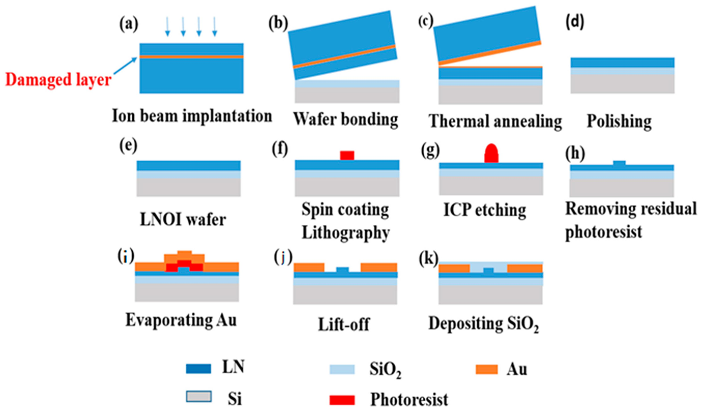
Turning LNOI wafers into functional chips involves a sequence of tightly coupled process steps: Material preparation → Wafer processing → Waveguide fabrication → Electrode integration → Testing → Packaging. Each stage directly affects final device performance and yield.
Waveguide fabrication
High-precision lithography and etching define the waveguide geometry that governs mode confinement, propagation loss, bending radius, and coupling efficiency. Surface roughness and dimensional uniformity are critical; even small process variations can increase optical loss and degrade consistency across the wafer.
Electrode integration
For electro-optic devices, electrodes must deliver strong field overlap with the optical mode while maintaining low microwave loss, proper impedance, and velocity matching. These parameters become especially important for high-speed modulators.
Device testing
Comprehensive characterization typically includes insertion loss, propagation loss, modulation bandwidth, extinction ratio, return loss, thermal behavior, and reliability metrics. Test protocols are adapted to the specific device architecture and application requirements.
4. Enabling Photonic Integration on TFLN
Photonic integration seeks to combine multiple optical functions on a single chip, reducing size, optical path length, and system complexity. TFLN supports a broad set of functions:
· Optical modulation — High-speed electro-optic modulators with low drive voltage and wide bandwidth.
· Phase control — Precise phase shifters for coherent systems, optical computing, and signal processing.
· Frequency conversion — Nonlinear devices for second-harmonic generation, parametric processes, and frequency shifting.
· Optical switching and routing — Electro-optic switches whose performance depends on speed, loss, and scalability targets.
· Microwave photonics — Integrated modulators and processors that handle high-frequency RF signals in the optical domain.
These capabilities make TFLN a flexible foundation for both discrete high-performance components and more complex photonic circuits.
5. From Single-Function Devices to Integrated Systems
True photonic integration requires more than co-locating devices on one chip. It demands compatibility among lasers, modulators, detectors, drivers, control electronics, and fiber or free-space interfaces. TFLN is frequently combined with other material platforms through hybrid or heterogeneous integration—pairing, for example, III–V lasers or silicon photonic detectors with TFLN modulators. While this approach leverages the strengths of each material, it also introduces process and packaging challenges that must be carefully managed.
6. Advancing Photonic Manufacturing
Scaling from laboratory demonstrations to commercial products hinges on manufacturing maturity:
· Process consistency — Uniform material properties and dimensional control across wafers.
· Yield optimization — Higher yields lower unit cost and enable volume production.
· Wafer-level processing — Parallel fabrication of many devices improves throughput and cost efficiency.
· Packaging and testing — Optical coupling, electrical interconnects, thermal management, and reliability screening often determine final module performance more than the chip itself.
Progress in these areas is essential for TFLN to move from research novelty to mainstream photonic component.
7. Application Landscape
TFLN-based photonics is relevant across multiple domains:
· High-speed optical communication — Modulators and related components for 800G, 1.6T and beyond.
· Optical computing — Electro-optic and nonlinear elements for photonic processors.
· Optical sensing and LiDAR — Precision modulators and frequency converters for specialized sensing architectures.
· Quantum photonics — Nonlinear sources and integrated circuits for quantum light generation and manipulation.
In each case, device design and process integration must be matched to the specific performance targets of the application.
8. Building an Integrated Photonic Value Chain
Successful deployment of TFLN technology requires coordinated progress across the entire value chain:
· Material & wafer — High-quality thin-film preparation and wafer engineering
· Photonic chip — Waveguide definition, electrode integration, and device fabrication
· Packaging & testing — Optical/electrical interfacing and rigorous verification
· Module & system — Assembly into application-ready optical engines
Only when these stages work together can the full potential of the platform be realized.
9. GLSUN and the Road Ahead
The rise of advanced photonic platforms is closely linked to broader advances in semiconductor and optical manufacturing. GLSUN’s positioning spans chips, devices, modules, and systems, enabling a holistic approach to photonic technology development. As TFLN and related platforms mature, the industry will need increasingly sophisticated capabilities in materials, fabrication, packaging, and system integration. Companies that operate across multiple stages of this value chain are well placed to explore emerging opportunities and accelerate the transition from laboratory results to commercial solutions.
Conclusion
Thin-film lithium niobate technology marks a decisive step in the evolution of integrated photonics—from bulk material to wafer-scale chip, and from discrete components to functional photonic systems. By combining the exceptional electro-optic and nonlinear properties of lithium niobate with modern thin-film waveguide engineering and manufacturing processes, TFLN provides a powerful platform for compact, high-performance photonic devices. As optical communications, computing, sensing, and quantum technologies continue to advance, the seamless integration of materials, chips, packaging, and systems will remain a central driver of innovation. From Material to Chip, From Chip to System — advancing the next generation of photonic technology through integration and engineering excellence.


