


Fiber Optic Tech
Comparing Four Technology Paths Shaping the Future of Compute Networks
In today’s era of rapidly advancing generative AI and large language models (LLMs), the interconnection efficiency of compute clusters has become a critical performance bottleneck. Traditional electrical packet switches (EPS), constrained by the latency and high power consumption introduced by repeated optical-electrical-optical (OEO) conversions, are increasingly revealing their limitations when handling massive data volumes.
In contrast, Optical Circuit Switches (OCS)—leveraging all-optical signal switching—are emerging as a key enabling technology for next-generation compute clusters adopted by tech giants such as Google and NVIDIA.
Paradigm Shift: From a “Busy Post Office”to a “Lightspeed Rail Yard”
To understand the advantages of OCS, it is essential to first clarify its fundamental difference from traditional electrical switches. Electrical switches (EPS) can be likened to a “busy post office”: every incoming data packet (letter) must be opened and processed by a processor (postal worker), which reads header information and determines routing. This constant signal conversion and processing introduces significant latency and consumes substantial electrical power.
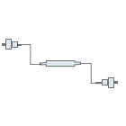
OCS, by contrast, resembles an “automated railway yard”. When a “train” carrying optical signals arrives, the system does not need to inspect its contents. Instead, it establishes a dedicated physical path by redirecting optical routes, allowing data to travel directly to its destination at the speed of light.
This architecture not only eliminates OEO conversion losses entirely, but also offers port-rate transparency—meaning no hardware replacement is required as bandwidth scales—significantly extending equipment lifespan and enabling seamless interconnectivity.
Four Technical Paths: A Diversified Competitive Landscape
Currently, the industry has developed four primary approaches to achieve optical path reconfiguration, each with distinct characteristics in terms of maturity, performance, and application scenarios:
MEMS (Micro-Electro-Mechanical Systems): The Dominant Mainstream Solution. MEMS technology is the clear market leader, accounting for over 70% of the market share.
Core Principle:
The system consists of fiber array units (FAUs) and MEMS micromirror arrays. Electrical signals precisely control micromirrors—typically hundreds of microns in diameter—to tilt in two dimensions. Using electrostatic comb-drive actuation and bias voltage adjustments, optical signals are directed to target output ports.
Key Advantages:
High technological maturity, excellent scalability, and an optimal balance between performance and cost.
Digital Liquid Crystal (DLC) / Liquid Crystal on Silicon (LCoS): A Reliable and Cost-Effective Option. This approach uses external electric fields to the alignment of liquid crystal molecules, thereby modifying the polarization state of incident light. Combined with polarization beam splitters, this enables optical switching.
Key Advantages:
No moving parts, resulting in very high reliability and relatively low production cost.
Key Limitation:
Slower switching speed, making it more suitable for static or semi-static scenarios with lower switching frequency requirements.
Direct Light Beam Steering (DLBS / Piezoelectric): Pursuing Ultra-Low Loss. This technology leverages the micro-displacement characteristics of piezoelectric ceramics under voltage control to directly adjust the spatial position and angle of fiber collimators.
Key Advantages:
Extremely simple optical path structure, enabling ultra-low insertion loss and high signal integrity.
Key Limitation:
As port count increases, precise alignment becomes more challenging, limiting scalability for large-scale systems.
Silicon Photonic Waveguides: A Future Star with Microsecond-Level Response
This approach defines optical routing paths on silicon-based chips, allowing light signals to propagate along preconfigured waveguide matrices.
Key Advantages:
Theoretically supports switching speeds at microsecond or even nanosecond levels and is highly suitable for ultra-high-density integration.
Key Limitation:
Challenges remain, including higher insertion loss, inter-channel crosstalk, and long-term reliability concerns. Large-scale commercialization is still in progress.
Three Key Application Dimensions of OCS in AI Compute Clusters
As AI models continue to grow in scale, OCS demonstrates irreplaceable value across three major dimensions:
Scale-Up (Vertical Scaling): Enhancing performance within a single node, such as increasing the number of GPUs per rack or boosting memory throughput. Google has successfully applied OCS in its TPUv4 clusters to optimize intra-node communication.
Scale-Out (Horizontal Scaling): Building large distributed clusters by adding more server nodes. In Google’s Jupiter architecture, OCS replaces traditional spine-layer electrical switches, significantly improving network flexibility.
Scale-Across (Inter-Data Center Scaling): Interconnecting geographically distributed data centers into a unified “super AI factory.” NVIDIA’s DCI solutions leverage OCS for efficient long-distance interconnectivity.
Conclusion and Outlook
With its inherent advantages of high bandwidth, low latency, and low power consumption, OCS has become a core driver in the evolution of AI networking infrastructure.
While MEMS currently leads the market due to its maturity and economies of scale, emerging technologies such as digital liquid crystal and silicon photonic waveguides are expected to play increasingly important roles in their respective niche domains as AI work""s demand higher switching frequency and integration density.
In this transformation toward lightspeed data transmission, OCS will continue to serve as the “power engine” of next-generation compute clusters.


